Why QFN Packaging Stands Out in Semiconductor Industry
1. Physical Advantages: Ultra-Thin and Compact
- Smaller Size: For example, a 24-pin chip in QFN packaging has a footprint 85% smaller than DIP and 60% smaller than SOP.
- Lightweight: QFN chips weigh only about one-tenth of a DIP package.
- High Packaging Efficiency: The ratio of chip area to package area reaches 0.3–0.5 (while DIP is only 0.05–0.1), making QFN packaging much more space-efficient.
2. Performance Advantages: Stable and Reliable
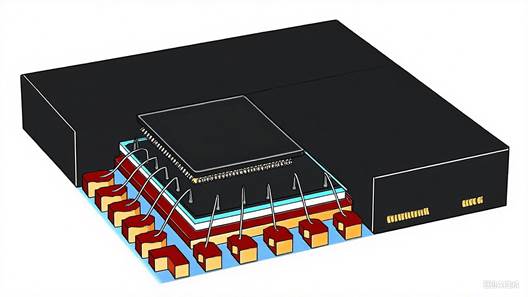
- Excellent Heat Dissipation: The large exposed thermal pad at the bottom is directly soldered to the PCB, and through thermal vias, heat is efficiently transferred to the ground copper layer.
- Superior Electrical Performance: Shorter conduction paths of QFN leads result in lower parasitic inductance and resistance, ensuring higher signal integrity.
- High Reliability: With a metal frame, precision etching process, and optimized molding compound, QFN packaging blocks moisture penetration, prevents delamination failures, and achieves better reliability than DIP, SOP, and even some BGA packages.
3. Cost Advantages: High Cost-Performance Ratio
- Although the unit price of QFN packaging is higher than DIP or SOP, the overall performance-to-cost ratio is currently the best in the market.
- Compared with BGA packaging, QFN costs about 30% less, and it is also about 15% cheaper than QFP.
- QFN packaging supports a wide range of process nodes, from 28nm mature nodes to advanced nodes, making it suitable for mid-range and high-end chips.
Typical Application Scenarios
QFN packaging is widely adopted in Bluetooth chips, PMIC power management ICs, audio chips, RF power amplifiers, and clock chips, among other applications.