
Why QFN Packaging is Ideal for Modern Chip Design | Compact, Efficient, and Reliable
Why QFN Packaging is Widely Preferred in the Chip Industry
The semiconductor industry value chain can typically be divided into three core areas: chip packaging and testing, circuit design, and wafer manufacturing, with chip packaging and testing falling into the backend of the industry chain. Among various types of surface mount packaging, QFN (Quad Flat No-Lead) packaging has gained significant popularity in the market due to its notable advantages.
Why do many chip design companies favor QFN packaging and use it extensively? We can analyze this from two main aspects: physical characteristics and quality performance.
(1) Physical Characteristics: Compact and Lightweight, Ideal for Miniaturization
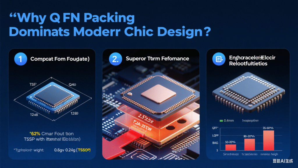
One of the most striking advantages of QFN packaging is its compact and lightweight design. The QFN package uses the same lead frame layout as TSSOP (Thin Shrink Small Outline Package), but the overall size is 62% smaller than TSSOP. This “small volume, lightweight” characteristic makes QFN packaging particularly suitable for applications where size, weight, and performance are all critical.
Currently, there is a clear development trend in the electronics industry: a continuous move toward more compact and lightweight products. Since the packaging volume of chips directly determines the chip’s weight, QFN packaging fits this trend perfectly.
(2) Quality Performance: Efficient Heat Dissipation and Excellent Electrical Performance
QFN packaging excels in thermal performance, thanks to its large-area heat sink pad at the bottom, which effectively dissipates heat generated by the internal chip during operation. However, in order to efficiently transfer heat from the chip to the PCB (Printed Circuit Board), the PCB also needs to be designed with matching heat sink pads and vias:
- The heat sink pad provides a stable and reliable surface for soldering.
- The heat vias provide an effective thermal path, transferring excess heat into the copper ground plane of the PCB. This copper ground plane absorbs the excess heat, greatly enhancing the chip’s overall thermal efficiency.
At the same time, the structural design of QFN packaging also ensures superior electrical performance, further enhancing its competitiveness in the market.