
Via-in-Pad Technology in PCB and Chip Packaging | Definition, Applications, Pros & Cons
Via-in-Pad Technology in Chip Packaging: Definition, Applications, Advantages, and Limitations
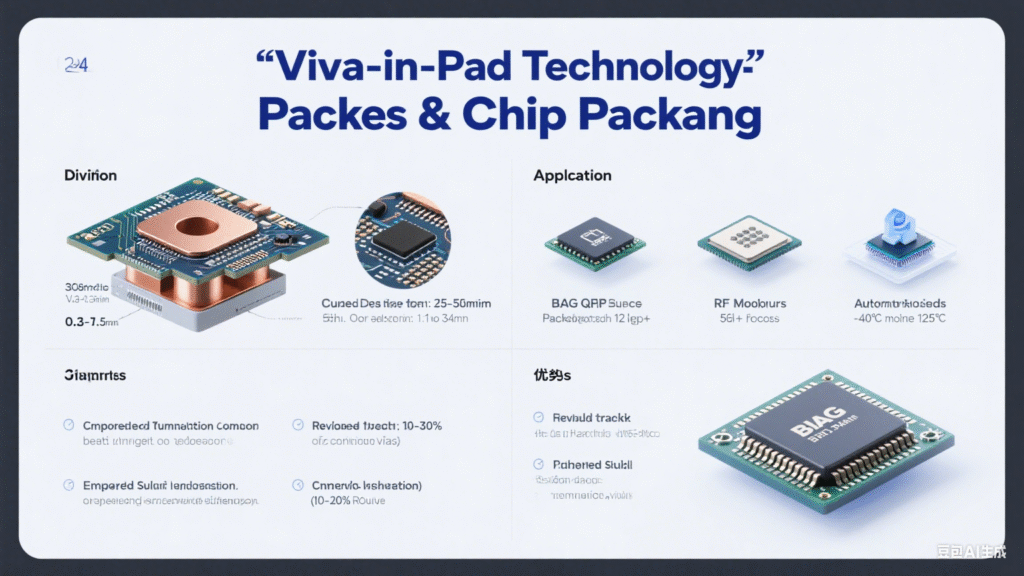
1. Definition and Classification of “Via in Pad”
“Via in Pad” refers to drilling vias directly on the surface-mount component pads in order to connect to internal PCB traces. The core purpose is to replace traditional fan-out routing or peripheral wiring by creating a direct connection channel from the component pad to the inner layer.
From a design perspective, via-in-pad enables higher component integration because it provides a direct path from device leads to the internal circuit, thereby optimizing PCB routing density.
In terms of classification, the rule is simple: regardless of whether the via’s inner diameter is located in the middle or on the edge of the pad, as long as the via’s outer diameter overlaps with the pad area, it is categorized as via-in-pad.
2. Typical Application Scenarios of Via-in-Pad
(1) BGA Routing Fan-Out
The stricter the product size requirements, the smaller the package sizes engineers tend to choose. For conventional BGA chips (pitch ≥ 0.65mm), there is generally sufficient routing space. However, when the IC pitch shrinks to 0.4mm, the air gap between pads is only about 0.15mm. In such cases, via-in-pad becomes a feasible routing solution.
For large BGA packages with pitch < 0.65mm, blind and buried via technology is usually required to achieve fan-out routing, making via-in-pad unavoidable.
(2) Space-Constrained PCB Design
In compact devices, via-in-pad may be introduced even for larger-pitch packages (e.g., 0.65mm) in order to save top-layer routing space and reduce negative effects of cross-layer routing.
(3) High-Frequency / High-Speed Circuits
In high-speed and RF designs, via-in-pad plays a critical role:
- It shortens the grounding path of RF components, reducing parasitic inductance and improving signal integrity.
- It allows ripples and noise to be conducted to the ground plane through the lowest impedance path, e.g., by placing vias directly under IC pads or capacitor pads.
- It also improves PCB thermal performance by enhancing heat dissipation through direct copper-plane connection.
3. Advantages and Disadvantages of Via-in-Pad
(1) Advantages
- High PCB Space Utilization – Reduces routing demand, improves trace density, and supports higher integration.
- More Stable Impedance – Minimizes via stub length, ensuring continuous impedance and reducing EMI issues. Shorter ground paths improve high-frequency performance.
- Improved Heat Dissipation – Direct connection to inner copper layers accelerates heat conduction and lowers thermal resistance.
- Cleaner PCB Layout – Fewer surface vias result in neater, more maintainable board design.
(2) Disadvantages
- Higher Risk of Solder Voids and Open Joints – During reflow, solder may wick into the via, leading to insufficient solder volume at the pad, voids, weak joints, or lifted leads. Small pad components are especially vulnerable. For this reason, designs where a via is located directly inside the top-layer solder pad must be avoided. Likewise, HDI structures such as “top pad → HDI via → short trace → HDI via → bottom pad” or overlapping HDI vias should also be avoided due to thermal concerns.
- Higher Processing Cost – Filling via-in-pad requires resin plug or copper plating, increasing PCB manufacturing difficulty and cost. For example, copper-filled vias must maintain flatness and thickness ≥15μm to ensure reliable solderability.
- Difficult to Inspect – X-ray cannot reliably detect voids inside filled vias. Residual bubbles or incomplete filling may still allow solder leakage, harming heat dissipation and long-term reliability.
- Difficult to Rework – Heat is quickly conducted away through vias, making desoldering and rework much harder. Nearby joints may also be unintentionally re-melted.
4. Summary and Key Takeaways
From the above analysis, the following core conclusions about via-in-pad technology can be drawn:
- “Do not use unless necessary.” Due to higher cost, via-in-pad should not be used if other lower-cost, mature alternatives exist.
- Effective in specific scenarios. Via-in-pad is highly beneficial in reducing loop impedance and improving thermal dissipation, making it suitable for high-speed/high-frequency circuits, compact PCBs, and fine-pitch BGA packages.
- If via-in-pad must be used, two rules apply:
- Avoid placing pads directly on both ends of the via.
- For double-sided soldering, strictly control reflow sequence and filling process, preferring copper-filled or resin plug + copper cap technologies to ensure reliable solder joints.