
Typical QFN Package Structures | Reliability & Soldering
Typical QFN Package Structures
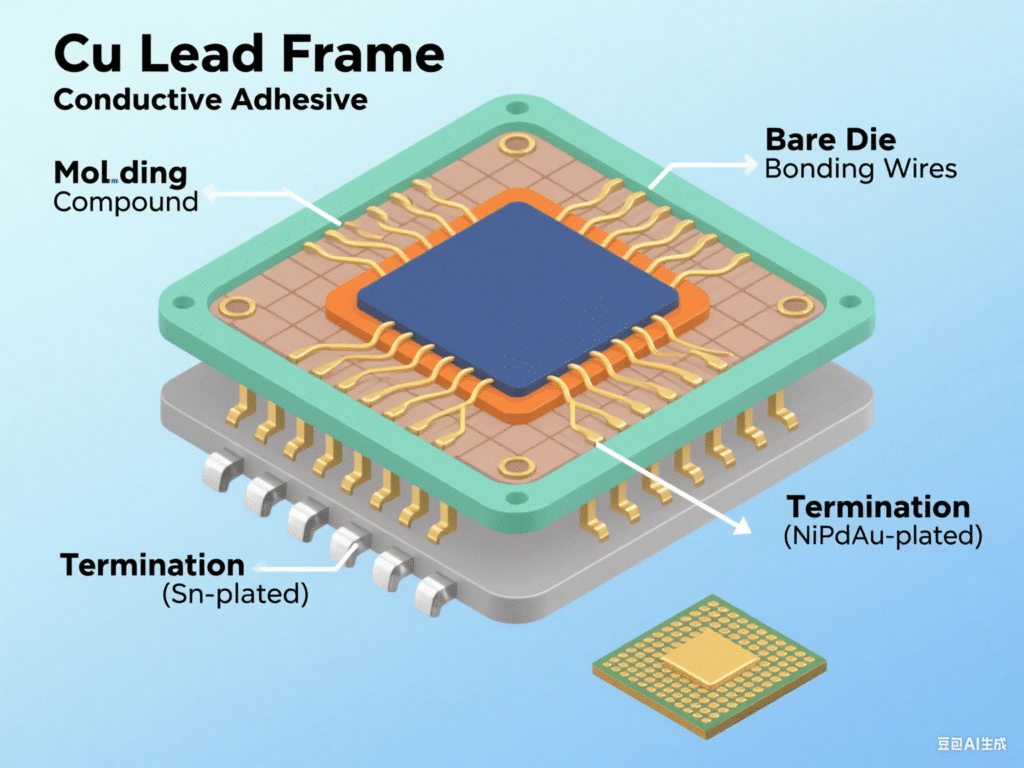
Plastic-molded QFN (Quad Flat No-lead) devices are mainly composed of a copper lead frame carrier, conductive adhesive, bare die, bonding wires, and the molded body. The solder terminals are generally located at the bottom of the package. The terminal surface finish is typically either Sn-plated or NiPdAu-plated, forming the standard structure of QFN packages.
QFN devices can be classified into two structural types based on the separation method: “punch singulation” and “saw singulation.”
- In the saw singulation type, the sidewall of the solder terminals is exposed bare copper. During subsequent screening and storage, the bare copper is prone to oxidation contamination. In severe cases, this oxidation can prevent proper solder wetting during assembly.
- In the punch singulation type, part of the solder remains on the terminal sidewall after stamping. However, since this residual solder is not an electroplated Sn layer and does not form a strong metallurgical bond with the copper lead frame, oxidation and contamination can also occur during storage and testing, leading to reliability concerns.
QFN packages can also be divided into two types according to whether the solder terminals are recessed: “recessed terminals” and “non-recessed terminals.”
Different terminal structures of QFN devices have a direct impact on subsequent assembly processes and solder joint reliability. This article focuses on analyzing the solder wetting behavior on QFN package sidewalls and its effect on solder joint reliability, providing valuable references for selecting typical QFN devices and achieving high-reliability assembly.