
QFN Side Pad Solder Wicking Study
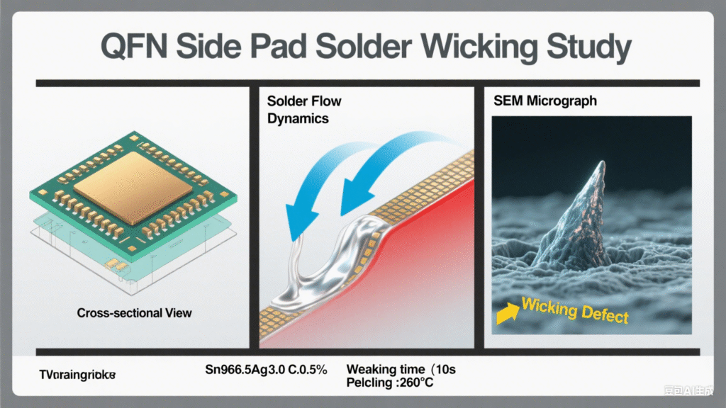
Because the side pads of QFN devices are exposed copper, they are highly prone to oxidation during the singulation process and subsequent storage. This oxidation reduces solderability and often leads to poor solder wicking on the side pads during assembly. Although current electronic assembly standards (such as IPC-A-610 and IPC-7093) do not specify solder wicking height requirements for side pads, military-grade electronics require QFN side solder joints to achieve at least 75% solder wicking height, with some customers even demanding 100% wicking to ensure stable and reliable electrical and mechanical performance.
1. Solder Paste Printing Quality
using Six Sigma analysis and two-level full factorial experimental design show that solder paste printing quality has the most significant impact on side pad solder wicking, followed by whether the QFN side pads are pre-tinned.
2. Side-Wettable QFN Packages
Improved QFN package designs with side-wettable terminations use special structural modifications and tin plating. These designs prevent issues such as exposed copper burrs caused by conventional “saw singulation,” ensuring good wetting angles. After soldering, joints can be inspected using AOI (Automated Optical Inspection), enhancing solder reliability and meeting high-reliability application requirements.
3. Chemical Pre-Tinning
proposed applying chemical tin plating to exposed copper surfaces after QFN singulation. This creates a solderable tin layer, and tests confirm that this method enables excellent wetting angles on side pads.
4. Dip-Tinning Pre-Treatment
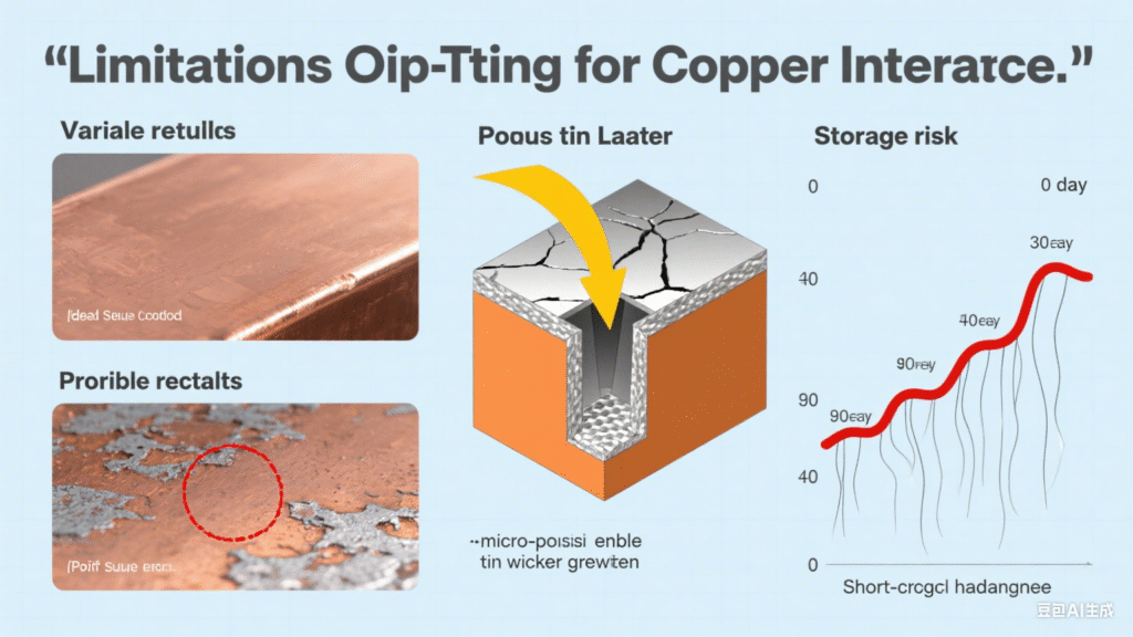
Some studies describe dip-tinning for pre-tinning bare copper interfaces. However, results vary depending on copper surface conditions. Poor-quality dip-tinning may leave some copper unsolderable, and porous tin layers can cause tin whisker risks during storage. Therefore, dip-tinning has limited applicability in practice.
5. Hand Solder Pre-Tinning
used manual soldering (iron-tinning) to pre-tin QFN side pads, analyzing delamination issues during soldering. Improvements include lowering soldering temperature and roughening the leadframe surface to enhance adhesion.
6. Flux Cleaning Treatment
To address oxidation-induced solderability issues, researchers compared iron-tinning, acid cleaning, and flux reflow cleaning. The flux cleaning method was selected as the optimal production solution, achieving 100% side pad solder coverage and over 96% joints with >75% solder wicking height. This significantly improves soldering yield for oxidized QFN devices.
7. Nano Solder Paste
Flux performance critically impacts solderability. Conventional solder pastes often suffer from particle agglomeration, leading to poor printing and soldering results. Nano-enhanced solder pastes (with nano-nickel, nano-copper, or other nanoparticles) improve wetting, oxidation removal, and uniform distribution of flux activity. This results in enhanced solderability and more reliable side pad solder joints.
8. Optimized Pad Design
proposed PCB pad and stencil design optimizations to address insufficient wicking height in QFN assembly. Recommended pad width is 0.25–0.50 mm, and pad length 0.60–0.96 mm. Pads should extend 0.1–0.2 mm outward and at least 0.05 mm inward, with minimum spacing of 0.2 mm from adjacent pads and thermal pads to avoid bridging defects.
9. Step Structure Design
Simulation studies show that introducing step structures on QFN terminations improves solder wicking. When the step depth ≥0.05 mm and width ≥0.02 mm, solder wetting and wicking height significantly improve, resulting in more reliable solder joints in final assemblies.