QFN Packaging Process Explained: Step-by-Step Guide
Front of Line (FOL) – QFN Packaging Early Stage
1. Wafer Incoming Quality Assurance (IQC) – First Optical Inspection
- Definition: Incoming wafers are inspected after unpacking to ensure quality before entering the production line.
- QA vs QC: QC ensures products meet required standards; QA builds the system to guarantee continuous compliance, creating trust internally and externally.
- Common IQC checks:
- Diameter (visual)
- Chipping (visual / caliper)
- Edge cracks (caliper)
- Pits & stains (visual)
- Scratches (microscope / caliper)
- Warpage & flatness (feeler gauge)
- Thickness (thickness gauge)
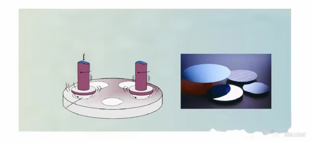
2. Wafer Backgrinding (BG)
- The wafer is mounted on a grinding chuck with vacuum suction.
- A rotating grinding wheel thins the wafer backside to the required thickness while DI water removes debris.
- Process:
- Apply protective tape on wafer front side.
- Grind backside.
- Remove tape and measure thickness.
- Common issues: grinding marks, chipping, TTV (Total Thickness Variation), water ingress.
3. Wafer Mounting (Dicing Tape Application)
Protective dicing tape applied before wafer sawing.
4. Wafer Dicing (Sawing)
- Wafers are fixed on blue tape to prevent die scattering.
- Diamond saw blade cuts along scribe lines.
- Defects: chipping, saw lane shift.
5. Second Optical Inspection
- Microscope inspection after wafer sawing to detect defective dies.
6. Die Attach (Die Bonding)
- Die picked up and placed on lead frame pad with epoxy adhesive.
7. Epoxy Cure (Baking)
- Curing in oven at 175°C for ~1 hour to remove stress.
8. Wire Bonding
- Gold or copper wires connect die pads to lead frame leads.
9. Third Optical Inspection
- Inspection after die attach and wire bonding.
End of Line (EOL) – QFN Packaging Back-End Process
10. Post-Mold Film Application
11. Molding (Encapsulation)
- Epoxy mold compound injected into mold cavity to encapsulate die and wires.
- Defects: voids, wire sweep, incomplete fill.
12. Post-Mold Cure
- 175 ± 5°C for ~8 hours.
- Purpose: strengthen structure, reduce stress.
13. Plating (Leadframe Electroplating)
- Pre-cleaning, acid treatment, copper pre-plating, silver plating.
- Defects: poor adhesion, burrs, incomplete plating.
14. Marking (Laser Engraving)
- Product ID, company logo, lot code.
15. Package Singulation (Sawing / Cutting)
- Packages cut into individual QFN units.
16. Final Optical Inspection
17. Packing & Shipment
- Electrical test, taping & reel, final packaging.