Flip-Chip Technology Explained: Definition, Advantages, and Applications in Modern Semiconductor Packaging
Flip-Chip Technology: A Comprehensive Analysis
This report provides a comprehensive and in-depth analysis of Flip-Chip technology, highlighting its critical role as a modern high-performance interconnect solution. It begins by examining the fundamental principles and process flow of Flip-Chip, along with its fundamental advantages over traditional wire bonding. It then explores strategic applications in high-performance computing (CPU/GPU), high-bandwidth memory (HBM), photonics (LEDs/CMOS image sensors), and micro-electro-mechanical systems (MEMS). Finally, it quantifies the improvements in electrical performance, thermal management, and system integration enabled by this technology.
1.1 Defining Flip-Chip: Beyond Wire Bonding
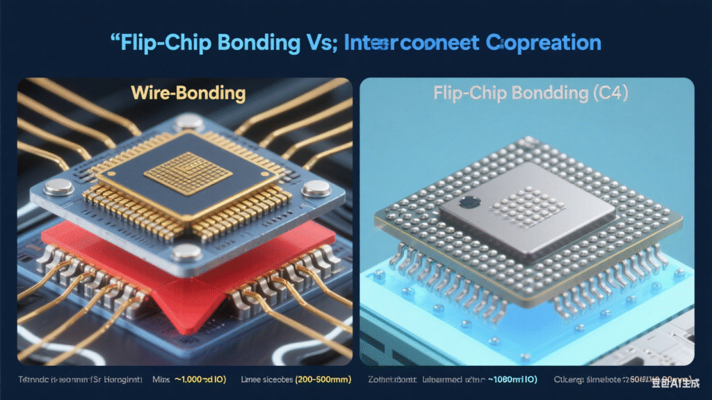
Flip-Chip technology, also known as Flip-Chip Bonding or its original name Controlled Collapse Chip Connection (C4), is an advanced semiconductor interconnect method. Unlike traditional wire bonding, where a chip’s active face points upward and connections are made through thin gold or aluminum wires, Flip-Chip flips the die face-down.
In this process, conductive solder bumps or copper bumps are fabricated on the I/O pads of the active surface of the chip. The chip is then flipped over so that these bumps align directly with matching pads on the substrate (PCB, ceramic substrate, or silicon interposer). Through reflow soldering or thermo-compression bonding, the bumps melt and form robust metallurgical connections.
This process simultaneously achieves both electrical interconnection and mechanical attachment. Originally developed in the 1960s for military and mainframe applications, Flip-Chip has since evolved into a mainstream choice for advanced packaging as transistor counts and I/O requirements surged.
1.2 Core Advantages: Density, Performance, and Miniaturization
The widespread adoption of Flip-Chip stems from its overwhelming advantages over wire bonding across several key performance metrics.
- Higher I/O Density – Unlike wire bonding, which is limited to chip perimeters, Flip-Chip allows area-array bump placement across the die surface, enabling thousands to tens of thousands of interconnects.
- Superior Electrical Performance – Flip-Chip’s short interconnect paths drastically reduce parasitic inductance and capacitance, minimizing delay, noise, and crosstalk. This makes it ideal for high-frequency, high-speed digital and RF applications.
- Enhanced Thermal Management – Metal bumps form a parallel heat-dissipation network. Additionally, the chip’s backside remains exposed, allowing direct contact with heat sinks or spreaders, which is critical for CPUs and GPUs with power consumption exceeding 100W.
- Miniaturization & Thin Profiles – By eliminating wire loops, Flip-Chip achieves lower package height and smaller footprint, making it well-suited for smartphones, wearables, and IoT devices.
Historically, the transition from wire bonding to Flip-Chip was driven by the I/O bottleneck created by Moore’s Law scaling. As transistor counts exploded, wire bonding’s perimeter limitation became untenable. Flip-Chip’s area-array solved this bottleneck and simultaneously provided better electrical and thermal performance.
2. Flip-Chip Interconnect Process Overview
The Flip-Chip assembly process involves multiple precisely controlled steps:
- Wafer Bumping – Deposition of under-bump metallurgy (UBM) and formation of solder or copper pillar bumps.
- Wafer Dicing – Cutting wafer into individual dies.
- Flip & Align – Flipping the die and aligning bumps with substrate pads.
- Reflow or Thermocompression Bonding (TCB) – Creating metallurgical interconnects.
- Underfill Dispensing & Curing – Injecting epoxy underfill to improve mechanical strength and thermal reliability.
- Encapsulation & Final Assembly – Adding molding compounds, heat spreaders, or lids.
- Inspection & Testing – Electrical validation and defect detection (X-ray, acoustic imaging).
3. Competitive Landscape: Flip-Chip vs Wire Bonding
- Signal Path & Performance – Flip-Chip’s micro-scale vertical interconnects provide unmatched signal integrity vs. long wire loops in wire bonding.
- I/O Density – Flip-Chip supports far higher I/O counts than wire bonding.
- Cost & Maturity – Wire bonding remains dominant in low-I/O, cost-sensitive applications. Flip-Chip is the mainstream solution for high-performance markets.
4. Strategic Applications
- High-Performance Computing (CPU/GPU) – Flip-Chip is the only viable solution for processors with thousands of I/Os and high power density.
- Advanced Memory & Heterogeneous Integration (HBM, 2.5D/3D Packaging) – Flip-Chip enables micro-bump interconnects for GPU-HBM integration via silicon interposers.
- Photonics (LEDs, CMOS Image Sensors) – Flip-Chip LEDs provide superior thermal efficiency, while CIS sensors leverage vertical integration for higher performance.
- MEMS & IoT Devices – Compact, robust Flip-Chip packaging supports high-density MEMS integration and rugged environments.