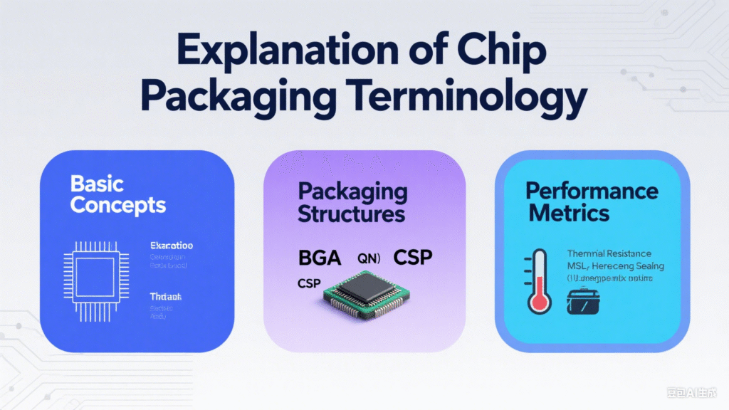
Explanation of Chip Packaging Terminology

Semiconductor Packaging Terminology Explained
1. Die Attach
- Definition: The process of attaching the die (chip) to a lead frame or substrate.
- Materials: Conductive adhesive (silver epoxy), insulating adhesive, solder, DAF (Die Attach Film).
- Requirements: Good adhesion strength, thermal conductivity, stress buffering.
- Equipment: Die Bonder.
2. Wire Bonding
- Definition: Connecting the chip pads to the package leads with metal wires.
- Materials: Gold wire (15–50 μm), copper wire, aluminum wire.
- Methods: Ball bonding, wedge bonding.
- Parameters: Bonding force, ultrasonic power, temperature, time.
3. Flip Chip Technology
- Principle: The die is flipped face-down and connected directly to the substrate through bumps.
- Bump Types: Solder bumps, copper pillar bumps, gold bumps.
- Advantages: Shortest interconnect, high I/O density, good heat dissipation.
- Challenges: CTE (Coefficient of Thermal Expansion) mismatch, underfill process.
4. Molding
- Purpose: Protects the chip and bonding wires from mechanical damage and environmental impact.
- Processes: Transfer molding, compression molding.
- Temperature: ~175 °C.
- Key Point: Avoid wire sweep, reduce molding stress.
5. Lead Frame
- Materials: Copper alloys (C194, C7025), Alloy 42.
- Processes: Stamping or etching.
- Surface Finish: Silver plating, NiPdAu plating, tin plating.
- Functions: Chip support, electrical interconnection, heat dissipation.
6. Substrate
- Types:
- Organic substrates: BT resin, FR4.
- Ceramic substrates: Alumina (Al₂O₃), Aluminum nitride (AlN).
- Metal substrates: Aluminum-based, copper-based.
- Layer Count: 2 to 16+ layers.
- Functions: Electrical interconnection, mechanical support, thermal management.
7. Underfill
- Purpose: Enhances reliability of flip chip solder joints.
- Materials: Epoxy resin with fillers.
- Processes: Capillary flow, pre-applied film, molded underfill.
- Functions: Stress buffering, moisture protection, adhesion reinforcement.
8. Die Saw / Dicing
- Methods: Mechanical sawing, laser dicing, plasma dicing.
- Blades: Diamond blades (20–35 μm thick).
- Requirements: Minimize chipping, cracking, contamination.
- New Technology: Stealth dicing.
9. Solder Ball
- Materials:
- Leaded: Sn63Pb37.
- Lead-free: SAC305 (Sn96.5Ag3.0Cu0.5), SAC405.
- Diameter: 0.1–0.76 mm.
- Processes: Ball placement, printing, electroplating.
- Inspection: Coplanarity, ball size, missing balls.
10. Reflow Soldering
- Temperature Profile: Preheat → Soak → Reflow → Cooling.
- Peak Temperature: ~250 °C for leaded solder.
- Atmosphere: Nitrogen (to reduce oxidation).
- Key Point: Prevent thermal shock, control heating rate.
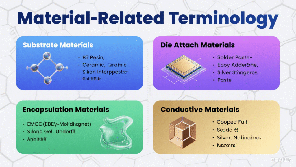
Material-Related Terminology
11. EMC (Epoxy Molding Compound)

- Composition: Epoxy resin + curing agent + filler (silica) + additives.
- Properties: Low stress, low moisture absorption, high glass transition temperature (Tg).
- Filler Content: 85–92%.
- Trend: Green EMC (halogen-free, antimony-free).
12. Die Attach Adhesive
- Types:
- Conductive adhesive: Silver-filled epoxy.
- Insulating adhesive: Pure epoxy.
- Solder: AuSn, SnAgCu.
- Performance Requirements: Low stress, high thermal conductivity, long-term reliability.
13. Solder Mask
- Function: Protects PCB circuits, prevents solder bridging.
- Colors: Green (most common), also black, white, blue, red, etc.
- Processes: Screen printing, photo-imaging.
- Thickness: 20–30 μm.
14. TIM (Thermal Interface Material)
- Types: Thermal grease, thermal pads, phase-change materials, liquid metal.
- Thermal Conductivity: 1–10 W/m·K.
- Applications: Between chip and heat sink.
- Requirements: Low thermal resistance, long-term stability.
15. Cu Pillar
- Structure: Copper pillar + solder cap (SnAg).
- Height: 40–100 μm.
- Advantages: Fine pitch capability, better electrical performance, resistance to electromigration.
- Applications: Advanced CPU/GPU flip-chip packaging.
16. RDL (Redistribution Layer)
- Function: Redistributes I/O pad locations to achieve fan-in/fan-out.
- Materials: Copper traces + polyimide dielectric.
- Line/Space: 2–20 μm.
- Applications: WLCSP, fan-out packages.
17. TSV (Through-Silicon Via)
- Definition: Vertical electrical interconnects through silicon wafers.
- Diameter: 5–50 μm.
- Aspect Ratio: 10:1 to 20:1.
- Applications: 3D IC, CMOS image sensors, HBM.
18. Interposer
- Materials: Silicon, glass, organic substrates.
- Functions: Connects multiple chips, enables high-density interconnect.
- Features: Contains TSV and RDL.
- Applications: 2.5D packaging, heterogeneous integration.
Testing & Reliability Terminology
19. MSL (Moisture Sensitivity Level)
- Levels: MSL1 (unlimited) to MSL6 (must be mounted within 6 hours).
- Standard: J-STD-020.
- Storage: MSL2+ requires dry pack.
- Baking: 125 °C for moisture removal if expired.
20. Delamination
- Definition: Separation at material interfaces.
- Locations: Die/EMC, EMC/lead frame, EMC/substrate.
- Causes: Moisture, thermal stress, contamination.
- Detection: Scanning Acoustic Tomography (SAT).
21. Wire Sweep
- Cause: Resin flow during molding displaces bonding wires.
- Consequence: Short circuits, open circuits.
- Prevention: Optimize wire loop profile, control molding parameters.
- Standard: Displacement < 1/3 of wire pitch.
22. Die Crack
- Types: Frontside crack, backside crack, edge crack.
- Causes: Mechanical stress, thermal stress, ESD.
- Detection: Optical microscopy, SAT.
- Impact: Functional failure, reduced reliability.
23. Solder Joint
- Quality Indicators: Wetting angle, fillet height, IMC (Intermetallic Compound) thickness.
- Defects: Cold solder, weak solder, head-in-pillow, voids.
- Reliability Tests: Thermal cycling, drop test.
- Failure Modes: Fatigue cracks, brittle fracture.
24. Thermal Resistance
- θJA: Junction-to-ambient thermal resistance (°C/W).
- θJC: Junction-to-case thermal resistance (°C/W).
- θJB: Junction-to-board thermal resistance (°C/W).
- Standards: JEDEC JESD51 series.
- Applications: Junction temperature calculation, thermal design.
25. CTE (Coefficient of Thermal Expansion)
- Unit: ppm/°C.
- Typical Values:
- Silicon: 2.6 ppm/°C.
- Copper: 17 ppm/°C.
- FR4: 15–17 ppm/°C.
- EMC: 8–20 ppm/°C.
- Impact: CTE mismatch causes stress and warpage.
26. Void
- Locations: Solder joints, underfill, die attach adhesive.
- Standard: Typically <25% of solder joint area.
- Causes: Flux outgassing, moisture, process control.
- Detection: X-ray inspection.
Dimensional Terminology
27. Pitch
- Definition: Center-to-center spacing of adjacent leads or solder balls.
- Trend: 1.27 mm → 1.0 mm → 0.8 mm → 0.5 mm → 0.4 mm → finer.
- Challenges: PCB manufacturing capability, soldering process.
- Impact: Determines I/O density.
28. Stand-off Height
- Definition: Distance between the bottom of BGA/CSP package and PCB.
- Typical Value: 0.1–0.5 mm.
- Impact: Affects underfill, cleaning, inspection.
- Trend: Decreasing height increases challenges.
29. Package Body Size
- Representation: Length × width × height (mm).
- Tolerance: ±0.1–0.2 mm.
- Trend: Continuous miniaturization.
- Standard: JEDEC defined standard sizes.
30. Die Size
- Representation: Length × width (mm or mil).
- Trend: Shrinking die area with process scaling.
- Pad Pitch: Affects packaging options.
- Scribe Line: Saw street width, 60–120 μm.
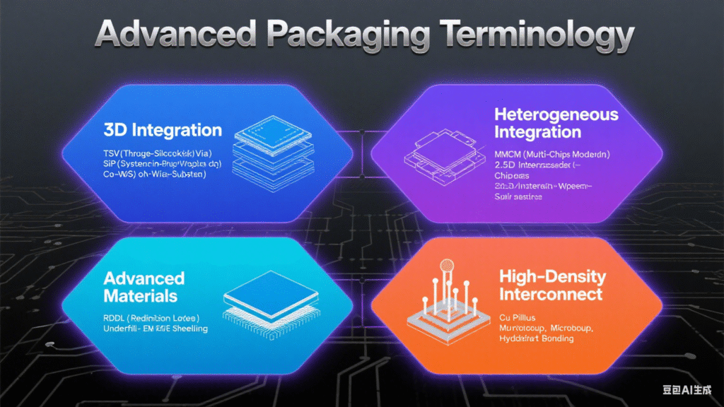
Advanced Packaging Terminology

31. 2.5D / 3D IC
- 2.5D: Chips placed side by side on an interposer.
- 3D: Chips stacked vertically and connected via TSVs.
- Advantages: High bandwidth, low power, small footprint.
- Challenges: Thermal management, testing, cost.
32. Fan-out Packaging
- Types:
- FOWLP (Fan-out Wafer Level Packaging).
- FOPLP (Fan-out Panel Level Packaging).
- Feature: RDL extends beyond chip footprint.
- Advantages: Substrate-less, flexible design.
33. Embedded Die Packaging
- Concept: Embedding chips inside PCB or substrate.
- Advantages: Ultra-short interconnects, good shielding, space saving.
- Process: Laser cavity, die embedding, lamination.
- Applications: RF modules, power modules.
34. Heterogeneous Integration
- Definition: Integration of chips with different technologies, functions, and materials.
- Examples: Logic + memory + RF + MEMS.
- Drivers: Beyond Moore’s law, system-level requirements.
- Technologies: Chiplet, 3D integration, SiP.
35. Chiplet
- Concept: Splitting a large chip into multiple smaller dies.
- Advantages: Higher yield, design reuse, mixed process integration.
- Interconnect: Standardized interfaces such as UCIe.
- Trend: Becoming a mainstream architecture.
