
DFN vs QFN Package Differences: Key Features & Applications
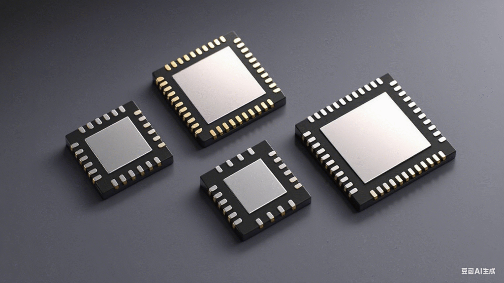
QFN (Quad Flat No-Lead) Package Overview
QFN is a leadless, surface-mount package available in square or rectangular shapes. It features:
- A large exposed thermal pad at the bottom center for heat dissipation
- Peripheral conductive pads around the thermal pad for electrical connections
- Typically lead-free solder structure with low inductance and capacitance
- Copper-based bottom material for superior thermal/electrical performance
- Compact size (2-7mm edge length)
DFN (Dual Flat No-Lead) Package Characteristics
DFN differs from QFN primarily in:
- Solder pads distributed on two sides (vs. QFN’s four-side pads)
- Ultra-thin profile (width <1mm)
- Pads located along the package perimeter (vs. QFN’s bottom-concentrated design)
Core Differences Between DFN and QFN
- Pad Distribution:
- DFN: Pads on two sides (rectangular shape)
- QFN: Pads on four sides (square shape)
- Thermal/Electrical Performance:
QFN’s copper-based bottom and central thermal pad enable superior heat dissipation, making it ideal for high-power applications. - Size & Applications:
- DFN: Used in 5G antennas, medical/industrial sensors, and LED drivers requiring high frequency/precision
- QFN: Preferred for power amplifiers, battery management ICs, automotive controls, and consumer electronics
SEO-Optimized Meta Description:
“Learn the key differences between DFN and QFN packages. Compare pad distribution, thermal performance, and applications for surface-mount leadless technologies. Ideal for engineers selecting components for 5G, automotive, or high-power electronics.”
Professional Terminology Preserved:
- Leadless package
- Exposed thermal pad
- Peripheral conductive pads
- Surface-mount technology (SMT)
- Low inductance/capacitance
This structured comparison clarifies technical distinctions while maintaining industry-standard terminology, optimized for search engine visibility.DFN vs QFN Package Differences: Key Features & Applications
QFN (Quad Flat No-Lead) Package Overview
QFN is a leadless, surface-mount package available in square or rectangular shapes. It features:
- A large exposed thermal pad at the bottom center for heat dissipation
- Peripheral conductive pads around the thermal pad for electrical connections
- Typically lead-free solder structure with low inductance and capacitance
- Copper-based bottom material for superior thermal/electrical performance
- Compact size (2-7mm edge length)
DFN (Dual Flat No-Lead) Package Characteristics
DFN differs from QFN primarily in:
- Solder pads distributed on two sides (vs. QFN’s four-side pads)
- Ultra-thin profile (width <1mm)
- Pads located along the package perimeter (vs. QFN’s bottom-concentrated design)
Core Differences Between DFN and QFN
- Pad Distribution:
- DFN: Pads on two sides (rectangular shape)
- QFN: Pads on four sides (square shape)
- Thermal/Electrical Performance:
QFN’s copper-based bottom and central thermal pad enable superior heat dissipation, making it ideal for high-power applications. - Size & Applications:
- DFN: Used in 5G antennas, medical/industrial sensors, and LED drivers requiring high frequency/precision
- QFN: Preferred for power amplifiers, battery management ICs, automotive controls, and consumer electronics
SEO-Optimized Meta Description:
“Learn the key differences between DFN and QFN packages. Compare pad distribution, thermal performance, and applications for surface-mount leadless technologies. Ideal for engineers selecting components for 5G, automotive, or high-power electronics.”
Professional Terminology Preserved:
- Leadless package
- Exposed thermal pad
- Peripheral conductive pads
- Surface-mount technology (SMT)
- Low inductance/capacitance