
Comparative Analysis of Plasma Cleaning Technologies in Wire Bonding: Batch vs. In-line Applications in QFN Packages
Comparative Analysis of Two Plasma Cleaning Technologies in Semiconductor Wire Bonding: Batch Type vs. In-line
In the semiconductor packaging process, particularly in wire bonding, pre-bond cleaning is a critical step that directly determines bonding reliability. Any residual organic contaminants, micro-particles, or metal oxides on the chip or wafer surface may lead to weak bonds, insufficient pull strength, shear test failures, and other quality issues, ultimately shortening the product’s service life.
Among the various pre-bond cleaning technologies, plasma cleaning has become the mainstream solution due to its efficiency and residue-free characteristics. Plasma cleaning is primarily divided into two technical routes:
- Batch Plasma Cleaning (Chamber-based)
- In-line Plasma Cleaning (Continuous Mode)
These two methods differ significantly in working principle, equipment configuration, processing mode, and applicable scenarios. This article presents a comprehensive comparison, from technical details to real-world applications, providing a valuable reference for packaging engineers in selecting the right technology.
1. Technical Principles and Equipment Structure
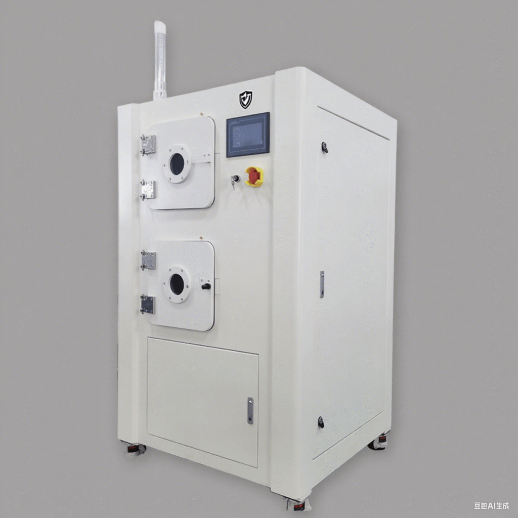
1.1 Batch Plasma Cleaning (Vacuum Chamber Type)
Core Principle:
This technology uses “batch plasma treatment under vacuum.” The wafers or chips are placed inside a sealed vacuum chamber, where an RF power source excites specific gases (O₂, Ar, N₂, etc.) to generate plasma. The plasma, consisting of free radicals, high-energy ions, and electrons, removes contaminants through:
- Chemical reaction: Free radicals react with organic contaminants, breaking them down into volatile small molecules (CO₂, H₂O).
- Physical bombardment: High-energy ions etch oxide layers and remove stubborn particles.
Equipment Structure:
- Vacuum chamber with symmetric RF electrodes
- MFC (Mass Flow Controller) for precise gas flow
- Vacuum pump system (0.1–10 Torr)
- Heating/cooling system to maintain optimal substrate temperature
Key Characteristics:
- Uniformity depends on chamber design and electrode layout
- Long cycle time (5–15 minutes per batch) but high overall throughput
- Flexible gas selection for targeted cleaning (O₂ for organics, Ar for oxides)
1.2 In-line Plasma Cleaning (Continuous Type)
Core Principle:
Unlike batch processing, in-line plasma cleaning is based on “continuous atmospheric or low-pressure plasma treatment.” Chips or wafers move along a conveyor or robotic track and pass through the plasma generation zone. Cleaning is performed in real time, without interrupting the production flow.
Equipment Structure:
- Linear plasma generation module (RF/microwave electrodes)
- Integrated gas supply system
- Motion control system to synchronize plasma with workpiece speed
- On-line detection (e.g., optical sensors) for real-time process adjustment
Key Characteristics:
- Operates in atmospheric or low-pressure environments (1–100 Torr)
- Extremely short treatment time (seconds per piece)
- High flexibility for small-batch or multi-product lines
- Well-suited for local area activation (e.g., pads, lead frames)
2. Core Differences Between the Two Technologies
| Dimension | Batch Plasma Cleaning | In-line Plasma Cleaning |
|---|---|---|
| Processing Mode | Batch vacuum treatment (multi-die) | Continuous online treatment (single/small batch) |
| Environment | High vacuum (0.1–10 Torr) | Atmospheric or low pressure (1–100 Torr) |
| Efficiency | Longer per cycle, high batch yield | Seconds per die, high-speed production |
| Uniformity | Chamber/electrode dependent | Module layout and motion control dependent |
| Cost | Higher (vacuum + RF system) | Moderate (simpler structure) |
| Maintenance | Higher complexity | Moderate, easier to maintain |
| Pollutant Handling | All types (organics, oxides, particles) | Mainly organics, mild oxides |
| Applications | Wafer-level packaging, DRAM/NAND, aerospace | QFN packages, BGA, small-batch production |
3. Practical Applications in Wire Bonding
3.1 Batch Plasma Cleaning Applications
- Wafer-Level Packaging (WLP): Removes organic residues and oxides before wafer dicing, ensuring high bonding strength.
- Multi-Die Stacked Packaging: Ensures uniform cleaning of all dies in DRAM, NAND flash stacks.
- High-Reliability Applications: Aerospace and automotive electronics requiring strict cleanliness and consistency.
3.2 In-line Plasma Cleaning Applications
- Die Cleaning Before Mounting: Common in QFN packages and BGA packaging lines to prevent weak bonding.
- Lead Frame Pretreatment: Removes copper oxides and enhances wettability for solder adhesion.
- Small-Batch/Custom Production: Ideal for RF devices, medical sensors, and IoT chips requiring fast switching.
4. Technology Selection and Future Trends
Technology Selection:
- Choose Batch Plasma Cleaning for high-volume production, wafer-level packaging, or when comprehensive cleaning is required.
- Choose In-line Plasma Cleaning for high-speed lines, flexible small-batch production, or QFN package assembly requiring localized cleaning.
Future Trends:
- Hybrid Cleaning Solutions: Combining batch pre-cleaning with in-line precision cleaning for optimized performance.
- Smart Control Systems: Real-time monitoring and adaptive parameter tuning to improve consistency and yield.
Conclusion
Both batch and in-line plasma cleaning technologies have unique advantages. The choice depends on production scale, contamination type, and packaging requirements. In the era of advanced semiconductor packaging and QFN packages, plasma cleaning has become indispensable for ensuring bonding reliability, yield improvement, and long-term device performance.