Chip Packaging Types Explained | QFN, BGA, CSP & More
1. DIP (Dual In-line Package)
Features: Leads extend from both sides in parallel rows and can be directly inserted into PCB holes.
Advantages: Easy manual soldering and replacement; high mechanical strength.
Disadvantages: Large size, not suitable for high-density assembly.
Applications: Early microprocessors and memory chips; now mainly used for prototyping.
2. SOP / SOIC (Small Outline Package / Integrated Circuit)
Features: Leads extend from both sides and bend outward for PCB surface mounting.
Typical Lead Pitch: 1.27 mm.
Advantages: 50–70% smaller than DIP; suitable for automated production.
Applications: Analog ICs, small-scale digital ICs.
3. QFP (Quad Flat Package)
Features: Leads on all four sides, gull-wing shaped.
Lead Count: 32–304.
Pitch Options: 0.8 mm, 0.65 mm, 0.5 mm, 0.4 mm.
Applications: Microcontrollers, DSPs, FPGAs.
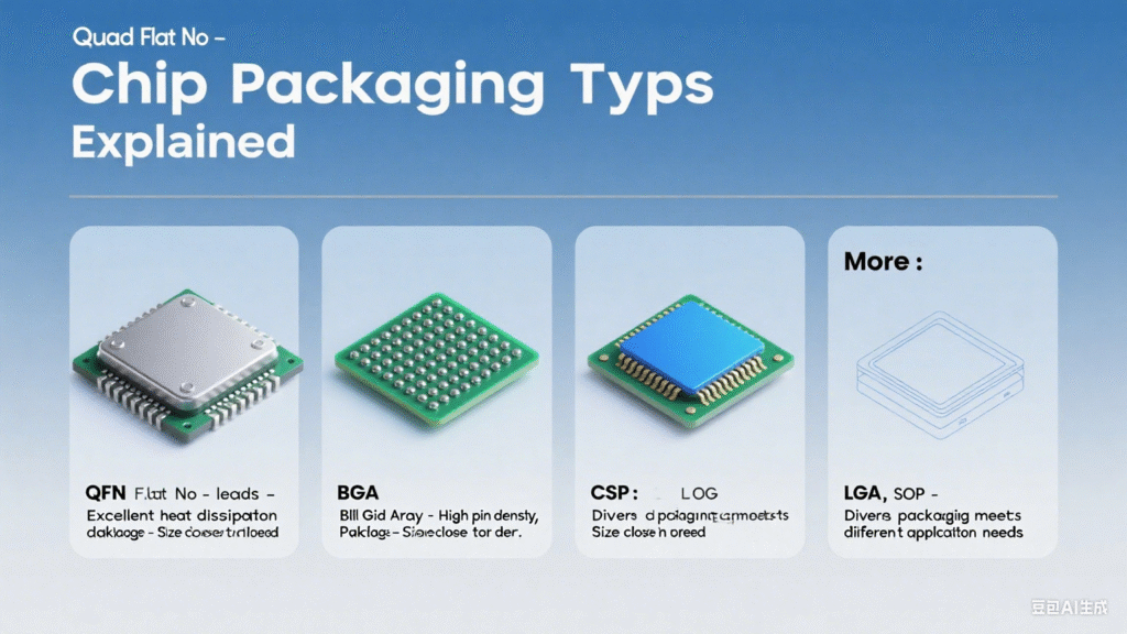
4. QFN (Quad Flat No-lead Package) –
Features: Pads located on the bottom side with an exposed thermal pad in the center.
Advantages: Compact size, excellent heat dissipation, and outstanding electrical performance with low parasitic inductance and resistance.
Applications: RF ICs, power management ICs (PMICs), Bluetooth chips, clock ICs.
👉 QFN packaging is one of the most popular and cost-effective semiconductor packaging solutions in modern electronics.
5. BGA (Ball Grid Array)
Features: Solder balls arranged in an array on the bottom side of the package.
Ball Pitch: 1.27 mm, 1.0 mm, 0.8 mm, 0.65 mm, 0.5 mm, etc.
Advantages: High I/O density, excellent electrical and thermal performance.
Disadvantages: Requires professional equipment for soldering and inspection.
Applications: CPUs, GPUs, FPGAs, large-scale ASICs.
6. CSP (Chip Scale Package)
Definition: Package size is no more than 1.2 times the actual chip area.
Features: Very close to the chip’s actual size.
Advantages: Minimizes package volume, improves electrical performance.
Applications: Mobile phones, wearable devices, and space-constrained products.
7. WLCSP (Wafer Level Chip Scale Package)
Features: Packaging is completed at the wafer level; final package size equals the chip size.
Process: Redistribution → Ball placement → Wafer dicing.
Advantages: Smallest size, shortest interconnection, efficient mass production.
Applications: Mobile RF switches, power management ICs.
8. SiP (System in Package)
Concept: Integrates multiple chips and passive components into a single package.
Advantages: Smaller footprint, shorter interconnections, higher system performance.
Technologies: Wire bonding, flip-chip, TSV, and others.
Applications: Smartphones, IoT modules.
9. PoP (Package on Package)
Structure: Two or more packages vertically stacked.
Typical Combination: Memory on top + Logic on bottom.
Advantages: Saves PCB space, shortens signal path.
Applications: Smartphone AP + DRAM integration.
10. FC-BGA (Flip Chip Ball Grid Array)
Features: Chip is flip-mounted directly onto the substrate, with solder balls at the bottom.
Advantages: Shortest interconnection path, best electrical performance, and superior thermal management.
Applications: High-performance CPUs, GPUs, AI processors.