3.5D Packaging for AI Training: Cost Reduction, Efficiency, and System Integration
3.5D Packaging Technology Helps Optimize AI Training Costs
In AI training scenarios, 3.5D packaging technology provides effective solutions for cost reduction across hardware design, manufacturing processes, energy consumption, and long-term operations. Its core advantages lie in transforming traditional packaging approaches and enhancing system-level efficiency.
I. Efficient Control of Hardware Design and Manufacturing Costs
1. Modular Architecture Reduces Development and Reuse Costs
3.5D packaging adopts a modular design, enabling the flexible integration of various functional modules required for AI training (such as CPU, GPU, and high-bandwidth memory HBM) into a single package.
This approach not only makes system configuration more flexible but also significantly reduces repetitive development investment.
The same set of chip modules can be recombined according to different AI application needs (e.g., deep learning training, inference acceleration), achieving cross-product reuse.
For example, AMD’s MI300A and MI300X accelerators are optimized for high-performance computing (HPC) and AI training respectively, while sharing core chip modules. This effectively shortens the product development cycle and reduces costs.
2. Chiplet Architecture Balances Performance and Cost
3.5D packaging breaks the limitations of traditional monolithic system-on-chip (SoC) design by decomposing it into multiple chiplets, then interconnecting them through advanced packaging technologies.
The key advantage is the ability to match different process nodes according to chiplet functions:
- Core compute modules → manufactured with advanced nodes (7nm, 5nm) for performance.
- I/O and control modules → produced with mature nodes (28nm) to reduce costs.
This balance satisfies AI training performance requirements while lowering total manufacturing costs.
3. Large-Scale Integration Improves Compute Cost-Efficiency
Through the combination of 3D stacking and 2.5D silicon interposer, 3.5D packaging integrates more compute resources within a limited package size.
This high-density integration not only boosts parallel processing capability for AI training but also lowers the cost per unit of computing power.
For instance, the MI300X accelerator integrates multiple GPUs via 3D stacking, increasing AI training throughput while significantly reducing cost per TOPS (trillion operations per second) compared to traditional packaging.
II. Precise Control of Power and Operational Costs
1. Low-Power Interconnects Reduce Long-Term Energy Consumption
3.5D packaging leverages copper-to-copper hybrid bonding, creating high-density and low-loss interconnects.
Compared with traditional micro-bump (μbump) technology, copper hybrid bonding reduces interconnect power consumption by over 30%.
For 24/7 AI training clusters, this not only cuts electricity costs in the long run but also lowers risks of equipment failure due to excessive power consumption, enhancing overall system stability.
2. High-Efficiency Design Reduces Cooling and Maintenance Costs
By tightly integrating functional modules and achieving low-latency interconnects, 3.5D packaging significantly improves system energy efficiency.
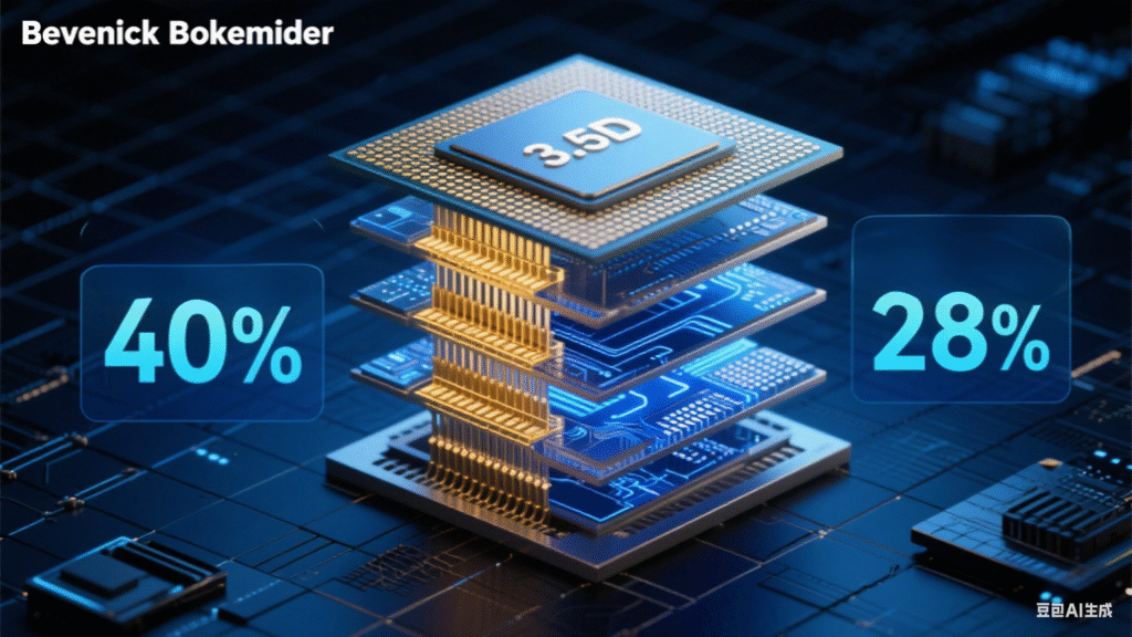
For example, the MI300X accelerator improves power efficiency by more than 40% compared with the previous generation in large language model (LLM) training.
Higher efficiency directly reduces power consumption, decreases cooling system demand, and eliminates the need for complex cooling equipment—thus lowering data center operating and hardware costs.
3. Unified Memory Architecture Reduces Hardware and Data Transfer Costs
Under the 3.5D packaging design, accelerators like MI300A enable CPUs and GPUs to share access to HBM memory.
This eliminates the traditional APU bottleneck, where CPUs use DDR memory and GPUs use HBM memory—causing delays and redundant data copies.
A unified memory architecture improves data flow efficiency in AI training, reduces the need for extra memory modules, and directly cuts hardware procurement costs.
III. System-Level Optimization Brings Comprehensive Cost Advantages
1. Tight Integration Simplifies System Architecture and Maintenance
3.5D packaging integrates CPU, GPU, and HBM into a single package, shortening communication distance, reducing data transfer latency, and simplifying overall hardware architecture.
This eliminates the need for complex external interconnects, reduces failure points, and lowers long-term maintenance costs.
2. High-Density Integration Saves Data Center Space Costs
By combining 3D stacking with 2.5D silicon interposer, 3.5D packaging delivers higher compute density within the same physical footprint.
For example, a server equipped with AI accelerators using 3.5D packaging can provide computing power equivalent to multiple traditional-packaged servers.
This means data centers can meet AI training demands without physical expansion, cutting costs on facility construction, rent, and infrastructure.
3. Fast Iteration Shortens Time-to-Market and Accelerates ROI
Thanks to modular and chiplet design, new products can be developed without redesigning the entire chip—only by adjusting chiplet combinations or upgrading certain modules.
This fast iteration capability shortens product launch cycles, enables companies to capture markets faster, accelerates return on investment, and reduces long-term R&D uncertainty.
Conclusion
3.5D packaging technology enables comprehensive cost reduction for AI training through optimized hardware design, power management, and system-level efficiency.
It not only extends the economic benefits of Moore’s Law (“higher performance, lower cost”) but also pushes beyond Moore by providing the core foundation for the next generation of high-performance, low-cost AI training platforms—driving scalable AI adoption across industries.